10W
Mini Audio Amplifier
An audio amplifier is an electronic device that increases the strength (amplitude) of audio signals that pass through it. An audio amplifier amplifies low-power audio signals to a level which is suitable for driving loudspeakers. The input signal of an audio amplifier may only measure a few hundred microwatts, but its output may be tens or even thousands of watts. Design parameters for audio amplifiers include gain, frequency response, distortion and noise.
Circuit
Diagram:-

Components
Used:
Resistances
R1
: 6 Ohm
|
R2
: 220 Ohm
|
R3
: 0.01 Kohm pontesiometer
Capacitances
|
C1
: 10uF / 25V
|
C2
: 100 uF / 16V
|
C3
: 100 uF / 63V
|
C4
: 0.1 uF
|
C5
: 0.1uf
|
C6
: 1uF
|
IC1
: TDA 2003
Speaker
|
Working:
Modifications:
This
be power amplifier circuit it work with high volt power supply about
125V directly. It composes UJT transistor and transistor the
ordinary. This circuit uses transformer sing bail with then apply to
high volt and use a loudspeaker has easy. It then get into trouble a
little. You can fine to decorate the popularity has of the sound with
VR1 – 1M. Read the detail adds in the circuit.

Applications:-
Important applications includes:-- public address systems,
- theatrical and concert sound reinforcement systems, and
- domestic systems such as a stereo or home-theatre system.
- Instrument amplifiers including guitar amplifiers and
electric keyboard amplifiers also use audio power amplifiers
Bomb
Game
Introduction:
This is a very common phrase in many movies when the action hero has a bomb in front of him with little time left and he has to choose which wire to cut and stop the bomb from exploding saving millions of people.
This game is just that... a count down timer and 4 wires of different colors.
The player has to remove each wire until it deactivates the bomb.
Circuit Diagram:

| Components Used: |
R2- 1K ohms resistor
R3- 560 ohms resistor
R4- 560 ohms resistor
R5- 4K7 ohms resistor
R6- 10K ohms resistor
R7- 10K ohms resistor
R8- 10K ohms resistor
R9- 10K ohms resistor
R10- 10K ohms resistor
C1- 10uF capacitor
T1- BC548 Transistor
T2- BC548 Transistor
Piezo- HPE-120 piezo
Digits- Dual 7 segment display - LTD6410G
IC1- 16F88 microcontroller from Microchip
S1- Push button
Others:
Box
PCB
Wires
4.8V Battery Pack
Hex program for the microcontroller
PCB
| Working: |
After the introduction, the message "S1" will appear on the display meaning that S1 needs to be pressed for the game to start.
All four wires must be plugged in. If one of the wires is not plugged in, the message "EE" will display meaning that an error occurred and the game will not begin.
As the game begins, the count down will start. The display shows the timer and 15 seconds is all the time we have to defuse the bomb.
There are four wires - red, green, blue and white. Unplugging them will simulate the cutting of the wire. Only one wire can be unplugged at a time and each wire can only be used once per play.
There are four actions possible - defuse the bomb, explode the bomb, increase timer speed and no consequence.
There is no need to change the color position because each position will correspond to a random action.
Every time a wire is unplugged, its action will be randomly given meaning that it's possible that even all of the wires will not defuse the bomb.
It's an original game and can bring a lot of fun to the kids.
For a final look it's possible to cut 3 pieces of PVC tube, paint them in red and glue the circuit on the tubes. This will make the traditional look of the dynamite bomb.
Digital
Mains Failure/Resumption Alarm
AC mains fails when over load is connected and this problem is common in now days. Here is the simple circuit using optocoupler Digital Mains failure and resumption alarm, for indicating AC mains fails or resumes by producing alarm sound.
Circuit Diagram:-

Components Used
Resistors (all ¼-watt, ± 5% Carbon)
R1, R4= 1 KΩ
R2, R5 = 10 KΩ
R3 = 22 KΩ
VR1 = 50 KΩ
VR2 = 47 KΩ
Capacitors
C1 = 0.22 µF
C2 = 1 µF/16V
C3, C4 = 10 µF/16V
C5 = 0.04 µF
C6 = 0.01 µF
C7 = 100 µF/16V
C8 = 470 µF/16V
Semiconductors
IC1 = MCT2E (optocoupler)
IC2 (N1-N3) = CD4011
IC3 = NE555 (Timer IC)
D1, D2, D3 = 1N4001
Miscellaneous
SW1 = SPDT (Single Pole Double Throw) Switch
SW2 = ON/Off Switch
LS1 = 8Ω/0.5W
9V Battery
Working
The circuit digital mains failure alarm is build around optocoupler. The resistor R1, capacitor C1 & C2, with diode D1 & D2 provide sufficient voltage to glow internal LED of optocoupler. Here the IC2 CD4011 is used as oscillator to generate low frequency of 0.662 Hz to 1.855 KHz controlling with preset VR1. Audio sound is generator by timer IC NE555 (IC2). The generated frequencies from IC2 vary from 472 Hz to 1.55 KHz controlling with preset VR2. For sensing mains fails position of switch SW1 to point 1 and for sensing mains resumption change the position of switch SW1 to point 2.
Alternative or Modification:
Here is a simple power resumption alarm circuit that can be fixed inside the switch box itself. It gives beeps when the power resumes after a power failure.
The alarm circuit uses a CMOS timer IC 7555 and a few components. IC 7555 is wired as a short duration monostable with its trigger pin 2 shorted to pin 6.So when the power is off, trigger pin is negative. When the power resumes after a break, output of monostable goes high and buzzer beeps. This keeps the Reset pin 4 high for a short period through D5. Capacitor C5 also help to keep the reset pin 4 till the output turns low. Then the capacitor C2 charges via R5 .
When the charge in C2 rises to 1/3 Vcc, trigger pin 2 becomes high and the output of monostable turns low. This takes around 30 seconds. For long duration beeps, value of C2 should be increased.When the output of monostable turns low, its reset pin 4 also turns low to inhibit the monostable from working.

Applications:
- To
Monitor Battery Chargers
- In
Hospitals
- In
Industries
- In
Schools
FM
Telephone Bug
The Telephone Bug is really a miniature FM radio transmitter broadcasting within the 88 to 108MHz band. It is designed to be wired inside a telephone or the wires leading to the telephone. The voice frequencies carried by the telephone wires modulate the FM transmitter allowing both sides of the telephone conversation to be heard on any standard FM radio. Because of the unique circuitry , no battery is needed to operate the unit. The power is taken from the telephone line.
Circuit Design:

Components Used:
Resistances:
R1- 12k
R2- 0.2k
R3- 1k
Capacitance:
C1- 330pF
C2- 470pF
C3- 12pF
C4- 25pF
Inductors
L1- 1uH
LED
Transistor- PNP A933
Antenna -15cm long 0.6 mm dia copper wire.
Bridge Rectifier
Working:
A simple telephone transmitter circuit that is ideal for transmitting the telephone conversation through small distances. The circuit is very simple and uses only few components. The entire circuit can be easily included in the telephone itself or in the junction box. The circuit is powered from the telephone line itself.
The transistor Q2 is wired as a a Colpitts oscillator to produce oscillations in the FM transmission band. The audio signal from the telephone line is coupled to the the base of Q2 to obtain the frequency modulation. The LED D1 acts as a power on indicator.
Applications:
- Can
be used for high frequencies communication.
IC
Tester
IC’s, the main component of each and every electronic circuit can be used for wide variety of purposes and functions. But sometime due to faulty ICs the circuit doesn’t work. Indeed it is lot tedious work to debug the circuit and confirm whether the circuiting is creating problem or the IC itself is dead. So to come up with these sorts of problems IC tester is designed.
Although ICs 741 and timer 555 are rare and expensive these ICs are frequently used ICs even by an average hobbyist and electronics students. They are very versatile and damage resistant too. Therefore we have designed the IC tester for timer IC 555 And Op-Amp IC 741
The tester described here test both the ICs [Timer 555 and Op-Amp 741] instantly. The circuit here uses only a few resistors, switches, sockets and capacitors which cost around $3 including the PCB and the 7-segment display. The tester we design is equally useful for a factory and the student of electronics.
Circuit Design:

Components Used:
Semiconductors
IC1-
555 Timer
IC2-
741 Op-Amp
D1,D2-
5mm LEDs
Display1-
FND507/LT542 Common Anode Display
Resistors
R1
12k
R2
68k
R3,
R4 10k
R5
to R12 - 1k
Capacitors
C1-
5uF, 16V electrolytic
C2-
47uF, 10V electrolytic
Miscellaneous
S1-
On/Off toggle switch
S2
DPDT miniature switch for mounting on PCB
BATT-
9-Volt, Battery
From the circuit diagram it is clear that the heart of this tester is the astable multi vibrator formed around 1C 555 which is approximately 2 Hz frequency. So, the output LED D1 (connected through link a and b snow in the circuit) blinks at a rate of 2 Hz if the IC 555 inserted in the socket works well.This output at pin 3 of IC 555 is also given through a DPDT (Double Pole Double Throw switch) to the pins2 and pin3 of IC 741 op-amp. The switch S2 selects the inverting or non-inverting input of the IC 741 . In this way the LED D2 ( connected through link c and d snow in the circuit) also blinks at of 2Hz rate if the IC 741 inserted is OK. If S2 selects inverting mode, then D1 and D2 blink alternately and if S2 selects non-inverting mode then D1 and D2 blink simultaneously. You may use 3V to 12V DC supply voltage safely. However, 9V DC is recommended.
More About circuit
As an interesting feature which gives a digital display without any confusion, you may use a common anode seven segment display. With op-amp IC 741 in inverting mode, the display shows 7 and 5 alternately. In the non-inverting mode it shows 9 and 0 alternately.
Common Anode display Configuration for connecting Display with circuit ( Please connect the A , C and B or D to the corresponding point in the circuit.:

Both, the two LEDs and digital display options are given circuit diagram. You can also use a common anode display having a damaged decimal dot and / or segment ‘e’ which are not used here
Common Cathode display Configuration for connecting Display with circuit ( Please connect the A and C to the corresponding point in the circuit.:
ou may also use a common cathode display here by just interchanging the connections of common cathode from positive to the negative of the supply on the PCB near the switch S2. Similarly, interchange the connections of R7 and R8 from negative to positive of the supply.
Motor
Protection
Introduction
A DC motor is
extensively used for industrial applications where a precise speed
control and a constant torque are desired. It is inversely
proportional to its field current. In case of field current failure,
the motor speed will rise to dangerously high level. A field failure
protection is therefore necessary to cut off the armature supply in
case of field current failure. It
could be assumed
that properly planned, dimensioned, installed, operated and
maintained drives should not break down. In real life, however, these
conditions are hardly ever ideal. The frequency of different motor
damage differs since it depends on different specific operating
conditions.Circuit Design:

Components Used
Resistors
R1- 5ohm, 25W
R2- 300ohm
All R- 20K, 25W
S- Shunt Regulator
Fuse
F1, F2, F3, F4 -1A
Diode
All- 1N4007
LED
Capacitor
C2, C3- N/O Contactor
All-200uF
Others
M- DC Motor
F1- Shunt Field
RE- Field Failure Relay
A1- Field Failure Relay
A2- Armature Ammeter
Working
The basic circuit of the field failure protection uses an ordinary 6V electromagnetic relay of the open type with I0 amps rated sturdy contacts. This relay can be used on a manual auto transformer-controlled DC drive and motorized or thyristor controlled drives. This motor has a shunt field current of 1.13 amps at 220V DC. A 5-ohm (25~watt) wire-wound resistor (R1) connected in series with the motor field produces a 5.6-volt drop across resistor (R1) as long as the field current exists, thus energizing the 6V DC relay connected across the resistor.
In case the motor field current fails due to any fault, the voltage drop across resistor (R1) will be zero which denergizes the relay (FFR) and cuts off the armature supply.
The circuit diagram of a manual aut0transfotmercontrolled DC drive of a 230V, 5HP DC motor with a separately excited shunt field of 230 volts ( l.l3 amps) and the FFR (field failure relay) circuit are shown in circuits diagram. When the start push button S2 is pressed, the contactor C is energized through S2 (N/O contact), limit switch S3 and stop push-button S1 contact).
The limit switch S3 is actually a part of the auto transformer, and it is so mounted that its contacts remain closed only when the auto transformer setting is at zero position. At all other settings of the auto-transformer, the limit switch contacts remain open. This is a safety device introduced, so that the motor can be started only from the minimum position of the auto-transformer setting, thereby starting at reduced voltage and current. If the motor is started on a high armature voltage, the starting current will be very high, especially if started on load, as is usually the case.
Modifications:
The diode bridge rectifier can be replaced by thyristor bridge rectifier for greater efficiency and for controlled rectification.
Applications:
- Protection
of DC motors.
- Also can be
used for AC motors too.
Nite
Rider Lights
As a keen cyclist I am always looking for ways to be seen at night. I wanted something that was a novelty and would catch the motorists eye. So looking around at my fellow cyclists rear lights, I came up with the idea of 'NITE-RIDER'. NINE extra bright LED's running from left to right and right to left continuously. It could be constructed with red LEDs for use on the rear of the bike or white LED's for an extra eye catcher on the front of the bike.
All IC's are CMOS devices so that a 9V PP3 battery can be used, and the current drawn is very low so that it will last as long as possible.
Circuit Design:

Components Used:
Semiconductors
IC1- 4027 flip flop.
IC2 and IC3- 4017 Decade Counter.
IC4- 555 timer.
IC5, IC6 and IC7- 4071 OR gate.
Resistances
R1 and R2- 10K resistors 1/4 watt
R3- 470 Ohm resistor 1/4 watt.
.Capacitor
C1 - 6.8uF Capacitor 16V.
Super bright LED's 1 to 9.
Battery- 9V PP3.
Switch- Single pole switch SW1.
Working
IC4, C1, R1 and R2 are used for the clock pulse which is fed to both the counters IC2 and IC3 Pin 14.
IC1 is a Flip Flop and is used as a switch to enable ether IC2 or IC3 at pin 13.
IC7a detects when ether IC2 or IC3 has reached Q9 of the counter pin 11.
IC5, IC6 and IC7a protects the outputs of the counters IC2 and IC3 using OR gates which is then fed to the Anodes of the
LED's 1 to 9.
Modifications:
Here in this previous circuit, we are using IC 555, Decade Counter and Flip flop. We can use a NPN transistor instead of a Flip-flop. The circuit diagram of which is given below.
Applications:
The Nite rider lights can be use in;-
- Bikes
- Cars
- Decoration
Purposes
Phone
Busy Indicator
Have you ever been using the modem or fax and someone else picks up the phone, breaking the connection? Well, this simple circuit should put an end to that. It signals that the phone is in use by lighting a red LED. When the phone is not in use, a green LED is lit. It needs no external power and can be connected anywhere on the phone line, even mounted inside the phone.
Circuit Diagram:

Components Used:
| Resistors | |
| R1 | 3.3K 1/4 W Resistor |
| R2 | 33K 1/4 W Resistor |
| R3 | 56K 1/4 W Resistor |
| R4 | 22K 1/4 W Resistor |
| R5 | 4.7K 1/4 W Resistor |
| Transistors | |
| Q1, Q2 | 2N3392 NPN Transistor |
| BR1 | 1.5 Amp 250 PIV Bridge Rectifier |
| LED1 | Red LED |
| LED2 | Green LED |
1. This is a very simple circuit and is easily made on a perf board and mounted inside the phone.
2. LED1 and LED2 flash on and off while the phone is ringing.
3. Do not worry about mixing up the Tip and Ring connections.
4. The ring voltage on a phone line is anywhere from 90 to 130 volts. Make sure no one calls while you are making the line connections or you'll know it. :-)
5. In some countries or states you will have to ask the phone company before you connect this to the line. It might even require an inspection.
6. If the circuit causes distortion on the phone line, connect a 680 ohm resistor in between one of the incoming line wires and the bridge rectifier.
Modifications:
In the previous circuit we were using two npn transistors and a bridge rectifier.
Here in this circuit we can make use of one FET transistors instead of two npn transistors. The circuit for this is given below.

POLICE
SIREN USING 555 TIMER
Introduction:
This circuit produces a sound similar to the police
siren. The two 555 timer acts as an atable multivibrator. The 555
timer IC is an integrated circuit used in a variety of timer, pule
generation and ocillator applications. The 555 timer can be used to
provide time delays as an oscillator and a a flip flop element. In
the beginning 555 is coupled like a low frequency oscillator so to
command the voltage at the second 555 IC at pin 5 which is a control
pin. The shifting of the voltage on pin 5 is the root of the second
oscillator frequency to get up and down.
Circuit
Diagram:

Components
Used:
Two 555 timer ICs
Resistors:
R1 = 68k
R2 = 68k
R3 = 8.2k
R4 = 8.2k
R5 = 10k
Capacitors:
C1 = 10uf,
C2 = 10uf,
C3 = 100nf,
C4 = 1uf
Diode- 1N4007
5 Volt Power Supply
speaker
Working
:
The police siren circuit explained here worked on NE555
timer IC. The circuit is build with the help of two NE555 IC which is
the basic block of this circuit. Both the timer IC in this circuit is
connected like a astable multivibrator. Although both the IC in the
circuit work at two dissimilar frequencies. IC1 is astable
multivibrator of slow frequency, works on frequency of 20Hz and
having
50% of duty cycle while IC2 is a fast astable
multivibrator works on frequency of 600Hz. IC1 output is then serve
to IC2 at the control pins. With the help of this arrangement IC2
output frequency will be modulated with the IC1 output frequency. The
circuit works on the DC supply between a range of 6V to 15V.
Modifications:
- The frequency range of the siren can vary with the exchange of R2 and R4 resistors with potentiometer.
- The pitch of sound can be enlarged with the attachment of the power amplifier at the output point.
Programmable
Electronics Dice Project
Introduction:
Dice
game is very interesting indoor game mostly played in childhood. Here
is verified game project programmable electronics dice useful in many
game. With the help of this project we can display any number between
1 to 9 according to our dip switch setting.
Circuit
Design

Components
Used
Resistors
(all ¼-watt, ± 5% Carbon)
R1 = 1 KΩ
R2 = 100 Ω
R3 – R7 = 4.7
KΩ
R8 = 220 Ω
Capacitor
C1 = 0.1 µF
Semiconductors
IC1 = 74LS13,
dual 4-input Schmitt trigger NAND gate IC
IC2 = 74LS191,
presettable binary counter with parallel facility
IC3 = 7474,
BCD-to-7-segmant decoder
Miscellaneous
DIS-1 = LTS542
common anode display of equivalent
SW1 = ON/OFF
switch
SW2 = 4-way dip
switch
Working
The project
programmable electronics dice comprises three ICs as heart and for
output a common anode display. Here, IC1 used is a dual 4-input
Schmitt trigger NAND gate IC where gate N1 used as frequency
generator which generate the clock frequency of 70kHz with the help
of resistor R2 and capacitor C1 and gate N2 load data at the input of
IC2. Where IC2 is a presettable binary counter with the facilities of
parallel loading. Lastly the output of IC2 is displayed on
common-anode, 7-segmant display with the help of IC3 which is
BCD-to-7-segmant decoder and the resistor R8 is used as current
limiter.
Setting for
the 4-way DIP switch for display range
| Dice Range | Close the inner switch | Open the inner switch |
| 1 to 2 | B and A | D and C |
| 1 to 3 | C only | A, B and D |
| 1 to 4 | A and C | B and D |
| 1 to 5 | B and C | A and D |
| 1 to 6 | A, B and C | D only |
| 1 to 7 | D only | A, B and C |
| 1 to 8 | A and D | B and C |
| 1 to 9 | B and D | A and C |
Ringing
Phone light Flasher
The project is designed to build an incoming phone ring flasher suitable for noisy environments. A phone line is connected through an opto isolator to drive a relay whenever telephone ring is detected by the circuit. The lamp flashes whenever there is an incoming call. This system is highly useful in a situation where there is lot of noise and it is not possible to listen the phone ring, such as a workshop, factory etc.
The phone line is connected to the circuit. This circuit is developed using an opto-isolator and an electromechanical relay to switch ON/OFF the lamp driven by a transistor.
Circuit diagram:
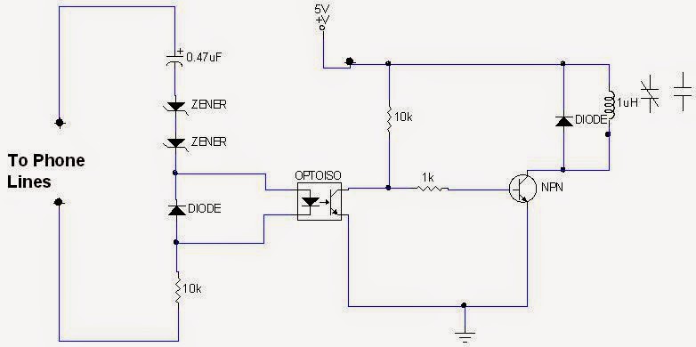
Components Used:
Resistors
R1- 10k
R2- 10k
R3- 1k
Capacitor
C1- 0.47uF
Semiconductors
Diode( D1 & D2)- 1N4007
NPN Transistor
Zener Diode
Opto-coupler
5V supply
5V Relay
Working:
When the telephone rings the line voltage rises to 72 volts. At this time the LED in the opto-coupler glows and the transistor conducts. Due to this the transistor Q1 conducts. This makes the relay ON. The load connected to the relay whether bulb or bell turns ON.
In the previous ciruit there was only light flashing on phone ringing. We can also apply some changes to the circuit. We can make use of both light and sound in the new circuit and it will be called as : Detect ringing signal tone with light and sound. The circuit for which is given below. The detect ringing signal tone circuit with light and sound.It is easy to use and good quality, Do not enter the power supply. Which as Detect ringing signal tone circuit Or ring tones on the telephone line, a signal incoming calls.
When an incoming call,When an incoming call, The C1, C2, will act as a coupling signal AC Volt to diodes D1, D2.Signal voltage is reduced down to approximately 10V.By D2 to detect, only a negative signal,One extreme to the other end of the wire loop.The D1 detect a positive signal, and the 4 LED. Flashing light attached to it,with frequency of the ringging tone.Which is about 20 Hz. and piezo speaker, show the audio beep .. beep, followed by a tone frequency of the ringing.
LED can be connected in series to increase, but less in proportion to the light.The circuit uses power from the telephone line.

Scoring
Game Circuit
Electronic number game circuit is an interesting game for children and elders or you can play with your friends. In this you have to perform mathematical operation like addition, subtraction, multiplication, division and in the end the person who has the highest score will win the game. A simple scoring game circuit that can be used for all occasions when a dice is needed.
Circuit diagram :

Components Used:
Resistors
R1- 10k
R2- 100k
R3- 1k
R4, R5- 0.560k
Capacitor
C1- 2.2uF
C2- 0.01uF
Semiconductors
IC1- NE555 timer,
IC2- 74LS192 counter,
IC3- 74LS247 decoder
Display- 7 segment LED display
Switches - SW1, SW2, SW3, SW4
5V Power Supply
Working:
The circuit is based on a NE555 timer,a 74LS192 counter,a74LS247 decoder and a & segment LED display. The timer IC1 will produce the clock for the counter IC(IC2) whose frequency is determined by R1 and C2.When S2 is pressed the IC2 will count in up mode and when S3 is pressed the IC2 will count in down mode. The IC 3 will decode the count to display it on the seven segment LED display . That is about the working of the circuit. The circuit is designed strictly sticking on to the basics of counters and is a good one for beginners. There is nothing big deal.
- To play the
game switch the power ON and press S1 to reset the counter.
- Now press S2
or S3 and release .The IC2 will hold the last count .Now press S4 to
see the score on display. That’s your score. Now the second person
can try.
- Each time
one tries, he should press the S1 to reset the count and then press
S2 or S3 and then S4 to see the score.
- Circuit can
be powered from a 9V radio cell or a 9V regulated DC power supply .
Modifications:
We can use a different circuit for scoring game circuit. The circuit of electronics number scoring game uses two timer ICs i.e. NE 555 (IC1 and IC3) to generate clock pulse and a decade counter to generate mathematical sign. A BCD counter followed by a seven-segment LED display driver is used to generate numbers. IC2 is a decade counter having ten outputs but here only four outputs are utilized. It is driven by clock pulse from IC1. When switch SW1 is on the set of LEDs ‘run’ so fast that all LEDs appear to glow at the same time. But when SW1 is off, only one set of LEDs glow showing a particular sign. Similarly, in FND500 display numbers o to 9 appear so rapidly that the display always shows 8 but when SW2 is off it shows a particular number from 0 to 9. The arrangement of LEDs to show the signs +, -, ×, ÷ is very important. It should be done according to figure “arrangement of LEDs”.

Speaker
to Microphone Converter Circuit
This circuit is a simple approach for converting a loud speaker into a microphone. Because microphones and speakers both function as electroacoustic transducers, you may use them interchangeably to an extent. Speakers are wired so that they do a better job sending audio out. Microphone wiring makes for optimal audio input. However, they both transmit sound in either direction. As a result, you may convert a speaker into a microphone in a pinch.
Circuit diagram:

Components Used:
Resistors:
R1- 220k
R2- 5.6k
R3- 2.2k
VR1- 0.10k
Capacitors:
C1, C2 - 220uF
C3- 100uF
Semiconductors:
T1, T2 – NPN Transistors
10V Battery
Working:
When the sound waves fall on the diaphragm of a speaker, there will be fluctuations in the coil and there will be a small proportional induced voltage. Usually this induced voltage is very low in magnitude and useless. Here in the circuit the low voltage is amplified using transistors to produce a reasonable output. The transistor Q1 is wired in common base mode and produces the required voltage gain. The transistor Q2 is wired as an emitter follower to produce enough current gain. The voice quality of this circuit will not be as much as a conventional microphone but quite reasonable quality can be obtained. To set up the circuit, keep the preset R2 at around 10 Ohms and connect the battery. Now adjust R2 to obtain the optimum sound quality.
Applications:
- Intercoms
- Walkie-Talkies
- Video game
voice chat peripherals
Touch
operated Band switch for Radio Set
Touch switch are now in vogue for stereo decks and other audio and video sets. This small circuit is meant for electronics enthusiasts to help them covert the manual band-switch of their radio set to an electronics touch switch with band indicators using LEDs.
Circuit Design:

Components Used:
Resistors (all ¼-watt, ± 5% Carbon)
R1, R2 = 3.3 MΩ
R3, R4 = 470 Ω
R5, R6 = 150 Ω
Capacitor
C1 = 0.1 µF
Semiconductors
IC1 = NE555
D1, D2, D3 = 1N4001
LED1, LED2 = different color LED
Miscellaneous
TP1, TP2 = Touch plate
RL1, RL2 = 6V, 100 Ω Relay
Working:
The circuit incorporates a 555 IC which operates in the biastable mode. Due to high input impedance presented by the threshold terminal (pin 6 of the IC) and the trigger terminal (pin 2), the timer can be set and reset with the touch of a finger.
Touching touch plate TP2 causes the output (pin 3) to go high. Hence relay RL2 gets energized while relay RL1 remains inactive. On touching TP1, relay RL1 conduct while RL2 is switch off.
If the relay are not switch on and off properly, the supply voltage may be increased to 7.5 volts. If it still doesn’t work, reduce the value of R3 and R4.
Applications:
- Radio broadcast.
Voltage
Stepper
In conventional voltage multiplier circuits, AC is used to charge the capacitors network via diodes in one cycle and discharge in the other cycle in a particular combination, which thereby produces multiples of the peak voltage. However, this circuit works on a different principle, and it is DC which is doubled. It can be used to power low current circuits.
Circuit Design:

Components Used:
Resistors (all ¼-watt, ± 5% Carbon)
R1 = 220 Ω
R2 = 6.8 KΩ
R3 = 68 Ω
Capacitors
C1, C2 = 0.01 µF
C3 = 0.1 µF
C4, C5 = 22 µF/40v
Semiconductors
IC1 = NE555
T1 = SL100
T2 = SK100
D1, D2 = 1N4001
Working:
IC555 is configured as an astable multivibrator producing rectangular pulses of about 10kHz frequency. Its output is made to drive the transistor pair T1 and T2. Transistor T2 being a pnp type, conduct when its base is negative, i.e. when the output of the IC produces a “low”. This charge C4 via diode D1 and ground (collector of T2 is grounded).
For the next pulse, i.e. when the output of IC is high, T1 conducts but T2 is cut-off, C4 cannot discharge because of diode D1. So the voltage across C4 and input voltage adds up and charge C5 via D2. Voltage across C5 will equal Vcc pulse voltage across capacitor C4 and Diode D1. Hence the operation.
However, it was found that if current greater then 50 mA and drawn, output voltage, hence regulation, is lost. Any DC voltage between 5V and 18V can be boosted (both voltage being the minimum and maximum range of the IC).
Modifications:
For better results, increase the value of C4 and C5 to 47 µF/40V.
Fire
Alarm using Thermistor & NE555
Introduction
A
fire alarm system is a set of electric/electronic devices/equipment
working together to detect and alert people through visual and audio
appliances when smoke/fire is present. These alarms may be activated
from smoke detectors, heat detectors, water flow sensors, which are
automatic or from a manual fire alarm pull station.
Circuit
diagram :

Components
Used:
Transisters:
T1: BC548
T2: BC558
T3:
SL 100B
Resistances:
R1- 470 ohm R2- 33
k-ohm
R3- 470 ohm R4-
560 ohm
R5- 47 k-ohm R6-
2.2 k-ohm
R7-
470 ohm R8-
470 ohm
Capacitances:
C1 is Polar Capacitaor
C2 and C3 are
electrolyitc Capacitor
C1: 10 uF
C2: 0.04 uF
C3: 0.01 uF
LED
DIODE:
1N4001
Thermistor
Speaker
555
IC
Working
A
thermistor is a type of sensor whose resistance varies significantly
with temperature, more so than in standard resistors. Thermistors are
widely used as inrush current limiters, temperatue sensors,
self-resetting overcurrent protectors, and self-regulating heating
elements. Thermistors differ from resistance temperature (RTD) in
that the material used in a thermistor is generally a ceramic or
polymer, while RTDs use pure metals. The temperature response is also
different
The
IC1 (NE555) is configured as a free running oscillator at audio
frequency. The transistors T1 and T2 drive IC1. The output (pin 3) of
IC1 is couples to base of transistor T3 (SL100), which drives the
speaker to generate alarm sound. The frequency of NE555 depends on
the values of resistances R5 and R6 and capacitance C2. When
thermistor becomes hot, it gives a low-resistance path for the
positive voltage to the base of transistor T1 through diode D1 and
resistance R2. Capacitor C1 charges up to the positive supply voltage
and increases the the time for which the alarm is ON. The larger the
value of C1, the larger the positive bias applied to the base of
transistor T1 (BC548). As the collector of T1 is coupled to the base
of transistor T2, the transistor T2 provides a positive voltage to
pin 4 (reset) of IC1 (NE555). Resistor R4 is selected s0 that NE555
keeps inactive in the absence of the positive voltage. Diode D1 stops
discharging of capacitor C1 when the thermistor is in connection with
the positive supply voltage cools out and provides a high resistance
path. It also inhibits the forward biasing of transistor T1.
Notes.
1]The
circuit can be powered from a 6V battery or a 6V power supply.
2]The
thermistor can be mounted on a heat resistant material like mica to
prevent it from damage due to excessive heat.
3]The
LED acts as an indication when the power supply is switched ON.
Modifications:
- We can use a buzzer instead of a speaker.
- We can use JFET's instead of transistors.
Wind Meter
A wind meter or an anemometer is a device used for measuring wind speed, and is a common weather station instrument.
Circuit
diagram:

Components
Used:
Resistances:
R1-
10 k
R2-
10 k
R3-
20 k
R4-
10 k
R5-
21.5 k
R6-
13 k
R7-
309 k
R8-
100 k
R9-
84.5 k
Capacitances
C1:
1uF
C2:
100 uF
IC1
IC2
Transistors
Q1= 2N4401
Q2= 2N4401
Q3= 2N3904
Power
Supply= 5V
Working:
A
wind meter or an
anemometer including a transistor in a transistor circuit with
suitable voltages applied thereto and a semiconductor diode connected
through resistors across the transistor. An output voltage is
obtained, representative of the velocity of the wind incident on the
anemometer, by taking the difference between the forward voltage drop
across the base-emitter junction of the transistor and the voltage
drop across the semiconductor diode. Here
is a very simple wind meter or anemometer circuit. The wind speed can
be measured up to 75m/s using this circuit.
The transistors Q1 and Q2 are used for sensing the wind. The relationship between thermal impedance of the transistor and the surrounding wind speed is utilized here. Transistors Q1 and Q2 are wired so that the Vce of Q1 is higher than Q2 and therefore there will be a higher power dissipation. The wind causes cooling and so the Vce of Q1 changes. The ends in different power dissipations and different voltages across R10.This variation is detected by the opamp and amplified to produce the Vout which is proportional to the wind speed. For still air Vout will be 0V and at 75m/s wind speed the Vout will be 2.5V. A 3V FSD voltmeter connected across the Vout terminal and ground can be used as the display.
The transistors Q1 and Q2 are used for sensing the wind. The relationship between thermal impedance of the transistor and the surrounding wind speed is utilized here. Transistors Q1 and Q2 are wired so that the Vce of Q1 is higher than Q2 and therefore there will be a higher power dissipation. The wind causes cooling and so the Vce of Q1 changes. The ends in different power dissipations and different voltages across R10.This variation is detected by the opamp and amplified to produce the Vout which is proportional to the wind speed. For still air Vout will be 0V and at 75m/s wind speed the Vout will be 2.5V. A 3V FSD voltmeter connected across the Vout terminal and ground can be used as the display.
Problems
with the Circuit
The sensor
transistors may latch up in a current rush mode, with the top Q1
fully on and current limited essentially only by the small sensing
resistor R4. Then Q1 can no more hold its temperature and the bridge
balancing fails.
Modifications:
We can use a differential amplifier. The base potentials of the cold reference Q2 and the hot Q1 are directly compared by the differential amplifier. Q2 is fed with a largely constant current determined by R1. The amplifier gain is basically R6/R5 resulting from its negative feedback. If the positive feedback is too large, then the circuit will go unstable or latch up, but this can be cured by increasing R4 or decreasing R6.
No comments:
Post a Comment